Research
The Heath lab works in the field of experimental solid state physics. We focus our attention on three materials systems: organic/inorganic composites for thermoelectrics, 2D materials, and thin-film photovoltaics. We’re also very interested in understanding and developing the capabilities of scanning probe microscopy.
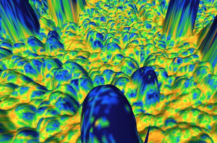
While physicists tend to want to investigate the most ideal systems, electronic responses can be strongly influenced by non-ideal features such as edges, surfaces, grain boundaries, and interfaces as well as defects like displaced atoms and impurities. Such features can sometimes cause unexpected responses that go beyond current physical models, and can provide interesting opportunities for applications. We’re particularly interested in using scanning electron microscopy and scanning probe microscopies to more deeply investigate the behavior of interesting material systems. We attempt to connect such microscopic observations to the larger macroscopic (“bulk”) properties.
Organic/inorganic composites for thermoelectrics
In composites, which consist of two dissimilar materials, how does the interface between the material affect electron transport and heat transport? How can this interface best be tuned to optimize the thermoelectric properties of the device? Can we create improved models of heat transport and electrical conductivity for such materials?
2D materials and devices
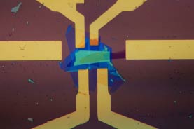
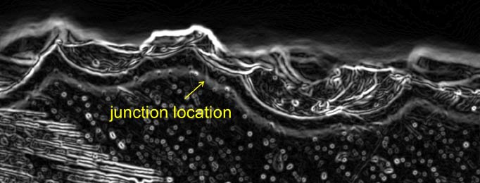
The "2D" materials are a whole family of materials that are stable as a single atomic or molecular layer; the most famous example is graphene. Not only can a single monolayer be isolated, but then different monolayers can be stacked together to create something entirely new. We’re working to develop techniques to create 2D devices that are accessible for researchers at small colleges like Reed, so that students can be immersed in this rapidly evolving field. We’re building field effect transistors and mapping out their electronic properties in the scanning probe microscope “in-situ”, while the device is actually operating. We’re especially interested in what may be going on along the one-dimensional edges and cracks in these materials, as well as at the interfaces between different materials. These are key locations where interesting physics may emerge. There are a vast number of questions to investigate about these systems, and this is an excellent platform for students to independently develop their own projects.
Photovoltaics (solar cells)
Low cost, thin film photovoltaic materials are typically polycrystalline, and contain grain boundaries, and other imperfections. When they absorb light, excited electrons are generated which move through the material to provide electrical energy. How do particular types of grain boundaries and imperfections affect the transport of free carriers, and ultimately the efficiency of the solar cell? Are some particularly detrimental and others benign?
Scanning probe microscopy
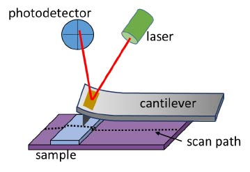
Scanning probe microscopy is both a valuable tool in the laboratory, and a platform for further investigation. Students are working to explore measurement parameters to refine and quantify results, and in the future we’d like to work to model probe/sample interactions and develop new measurement approaches.