Tags
"electronics"
Insights at Sigenics, Winter Externship, Edgar Perez
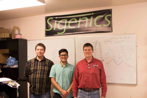
This winter, two fellow Reedies and I had an amazing experience working with Dr. Doulas Kerns and Mr. Marcus Snyder at Sigenics. Together, they provided an empowering three day externship and enlightening insights as to the life of electrical engineers. We started our trip with an hour long commute from the California coast to the base of Mt. San Antonio. Relieved from traffic by the carpool lane and good music, our trip to Sigenics was always pleasurable.
We spent our first day learning about the company and the different roles of scientists and engineers. Dr. Kerns started off with a small tour of their lab and showed us some of their designs. He really blew us away when he showed us the incredibly small size of their circuit designs and their circuit elements. A chip no bigger than 1 squared millimeter can house billions of transistors. As if hearing about this wasn’t enough, Dr. Kerns pulled out a sample of their work and placed it under and a powerful microscope. There is was. Mind-numbing in scale and constructed with jaw-dropping precision. Millions of components carefully embedded in a tiny silicon chip, and the chip: even more precisely designed. Yet here we were, three unexperienced undergrads sharing a room with the chip designers themselves!
The relationship between an engineer and a scientist was the next item on Dr. Kern’s agenda. Using a very Reed-esque analogy of a pizza shop, he demystified some of the quirks of engineering. The relationship between engineers and scientists is actually more symbiotic in nature than one would expect, he explained. Engineers use scientific results to develop tools for scientists. In turn, scientists use the tools to develop new results. This is relationship is a vertical growth pattern where the two fields help propel one another. Along the way, the tools and results produced by both parties will spread horizontally, manifesting themselves as new technologies or constructions for the benefit of our societies. We ended the day with a scientific investigation of the phenomena occurring “behind the scenes” in the electrical components we used the following day, and (appropriately) some delicious pizza from a local shop.
Continue reading Insights at Sigenics, Winter Externship, Edgar Perez
Sigenics Winter Externship, Farhanul Hasan
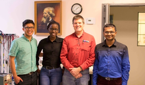
On the 11th of January, 2015, I landed in the Los Angeles international airport for a work experience opportunity that I had been looking forward to ever since my application was accepted. I was picked up by Edgar, who was also doing the externship, and Jackie (Edgar’s sister), whose generosity allowed us accommodations for the duration of the program. Jackie drove us to her house in Costa Mesa and Modi, another of the externs, came in later in the evening. We went out to grab dinner and buy groceries for the next few days.
Day 1: Jan 12
We woke up at around 6:30 and hit the road at 8:15. The traffic wasn’t nearly as bad as we expected and as a result, we reached Sierra Madre by 9:15. At the Halcyon building (which housed the Sigenics Lab), we were greeted by our sponsor, Dr. Douglas Kerns. We went inside the Sigenics lab and met Marcus Snyder, the office manager and senior technician. Douglas gave us a brief overview of the company and its goals. We learned that Sigenics specializes in designing integrated circuits (IC) and silicon wafers among their microelectronic components. Douglas also explained the science behind electronics and electric circuits. After learning these introductory ideas, we looked at a silicon wafer chip through an electron microscope, which was very exciting as we could actually see the arrangement of electrons that serve as the building blocks for all of electronics.
Continue reading Sigenics Winter Externship, Farhanul Hasan